The COVID-19 pandemic and the global chip shortage resulted in no new GPU announcements in 2020. NVIDIA finally announced the new A100 80GB in November 2020. It is built on top of NVIDIA’s Ampere architecture, with their HGX platform fuelling the vision of the AI supercomputing revolution. It has nearly double the memory bandwidth when compared to the previous generation of Volta cards and is the direct successor to the V100 based on NVIDIA’s Volta architecture. It aims to provide deep learning engineers and research scientists with the ability to perform cutting-edge research using the best hardware on the market with greater memory bandwidth. This will allow them to process larger datasets and make more accurate predictions.
The NVIDIA A100 80GB GPU is available in the NVIDIA DGX systems. System integrators like Dell, Gigabyte, HP, Supermicro, Lenovo, and Atos, provide systems equipped with HGX A100 integrated baseboards in configurations allowing four to eight GPU(s) to be connected. But does it live up to the hype?
Here’s everything you need to know about the NVIDIA A100 80GB.
What is the NVIDIA A100 80GB?
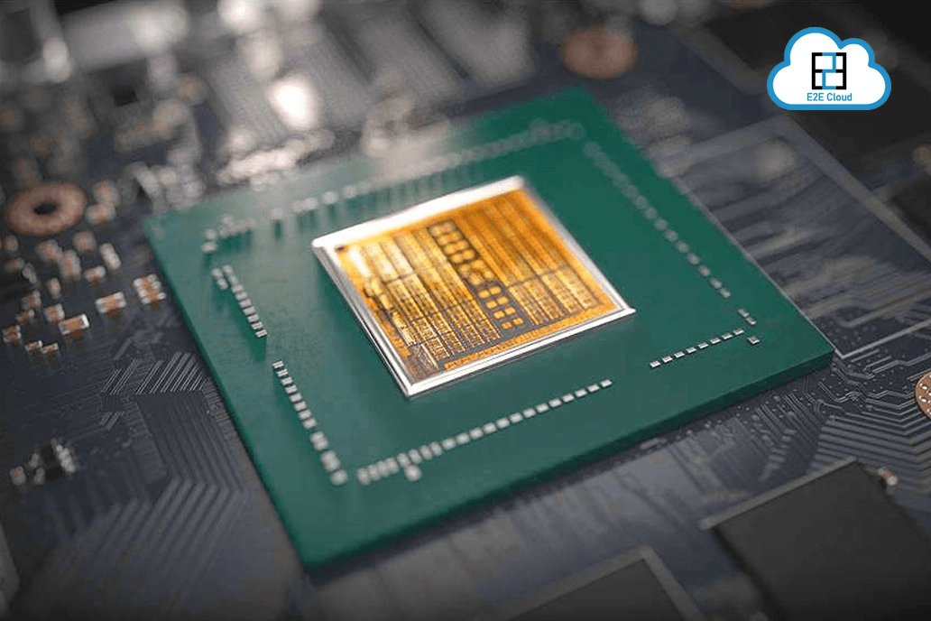
The A100 80GB is NVIDIA’s latest offering, the most powerful computing accelerator globally. It is a dual-slot PCI Express card, based on NVIDIA’s Ampere architecture and manufactured using TSMC’s 7-nanometer process. Ampere offers significant advantages with NVIDIA’s third-generation tensor cores, bringing training time down from weeks to hours. With built-in support for Multi-Instance GPU (MIG), a GPU can be partitioned into multiple GPU instances, each of which has its high-bandwidth memory and cache and computing processors. It makes for the perfect, well-rounded package with support for NVLink, structural sparsity, and second-generation RT(Ray Tracing) cores.
The A100 80GB expands on the numerous capabilities of the A100 40GB, making it appropriate for a wide range of applications with massive data memory requirements. The chip aims to assist companies in making quick decisions using real-time data analysis. Given the gigantic memory bandwidth requirements, the ability to perform real-time data analysis is no mean feat. Memory bandwidth is still one of the most crucial factors for advancing artificial intelligence/machine learning (AI/ML) processing. The A100 80GB aims to deliver on that front by offering a massive 2 TB/s memory bandwidth using Samsung’s HBM2e.
A100 80GB: The Core Advantages
- MIG technology: It has the ability to split a single A100 into up to seven separate GPU instances, each with its high-bandwidth memory, cache, and compute cores, using Multi-Instance GPU (MIG). Breakthrough acceleration is now available for any application, large or little, with an assured guarantee of excellent service. Furthermore, IT managers can provide GPU acceleration appropriately sized for each user and application to ensure maximum efficiency.
- Structural Sparsity: With millions and even billions of varying parameters, AI models can be extremely challenging to navigate through. Given that not all of these parameters make sense, structural sparsity leaves the parameters that do not affect the results out of the calculation, boosting performance by over 2x.
- HBM2e GPU Memory: The A100 80GB boasts double the memory capacity of its predecessor and an industry-first 2 TB/s memory bandwidth, which is the best in the industry. When coupled with higher DRAM utilisation efficiency, it can help you power through most workloads with ease and grace.
- Third-Generation Tensor Cores: The all-new, third-generation tensor cores provide up to 20 times the AI throughput compared to the previous Volta generation with the introduction of the new TF32 format. This is more than twice the throughput for high-performance computing, and 20 times improvement in INT8 for AI inference and support for the legacy BF16 data format. Artificial intelligence (AI) models are becoming significantly more complicated as they tackle complex problems, such as conversational AI or autonomous vehicles. The tensor cores can reduce training times, providing your team with more time to test and improve models.
- Third-Generation NVLink and NVSwitch: With a throughput of up to 600GB/s delivered by NVIDIA NVLink in the A100 80GB, it is two times greater than the previous generation. This allows for the best potential application performance on a single server. NVLink allows two NVIDIA A100 PCIe boards to be bridged, with numerous pairs of NVLink connected boards being housed in a single server.
How Much Does it Cost?
The NVIDIA A100 80GB Tensor Core GPU provides unmatched acceleration to drive the world’s most performant, dynamic data centres for AI, big data, and high-performance computing (HPC) applications. By promising to deliver over twenty times the performance of cards based on their previous Volta architecture, NVIDIA ensured that these things fly off the shelf quicker than they could resupply. Given the complexities of enterprise boards, the pricing structures can vary a lot, but a single A100 80 GB retails for somewhere around $15,000.
For a Free Trial: https://bit.ly/freetrialcloud


